


Intel’s Cutting-Edge Semiconductor Packaging: A Pillar of Foundry Excellence
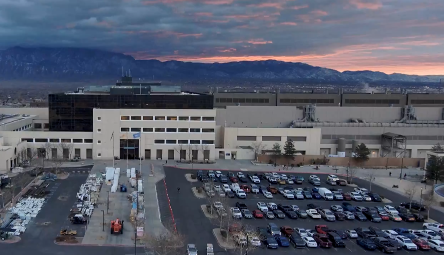
Intel’s Rio Rancho Facility
intel
The Growing Significance of Advanced Semiconductor Packaging
The semiconductor sector is undergoing a essential change where refined packaging techniques are becoming as crucial as the chip fabrication process itself. intel, a veteran in semiconductor innovation, has placed advanced packaging at the core of its foundry strategy. while much attention has been given to Intel’s progress with cutting-edge nodes like intel 18A and the forthcoming 14A, it is indeed thier mastery in refined packaging solutions that truly distinguishes them within today’s fiercely competitive market.
Revitalizing Innovation: The Rio Rancho Campus
Spanning an notable 218 acres, Intel’s Rio Rancho site exemplifies both heritage and forward-thinking innovation. Established in 1980 and once ranked among the globe’s most sophisticated fabs by the early 2000s, this facility experienced a period of dormancy before being rejuvenated under Intel Foundry’s vision focused on advanced semiconductor packaging. presently, it stands as one of America’s leading integrated hubs for manufacturing and testing complex components while maintaining ample capacity for future expansion.
A recent milestone at rio Rancho includes launching silicon photonics production tailored for external clients-highlighting Intel’s dedication to broadening its foundry offerings. Additionally, this location is set to lead global volume manufacturing of glass substrates-a technology still largely confined to pilot phases elsewhere-cementing its position at the forefront of next-generation assembly methods.
A Global Network Driving Packaging Innovation Forward
intel operates multiple specialized sites worldwide dedicated exclusively to advanced packaging technologies such as Embedded Multi-die Interconnect Bridge (EMIB) for efficient die-to-die communication in complex multi-chip modules and Foveros technology enabling vertical stacking through fine-pitch interconnects.These innovations facilitate higher performance densities without relying solely on transistor miniaturization-a critical advantage given Moore’s Law approaching physical limits.
this extensive footprint includes key locations like Chandler (Arizona), Penang (Malaysia), New Mexico (Rio Rancho), Oregon, and Malaysia-all integral for volume assembly and rigorous testing operations that demand adaptability amid evolving customer requirements.
The Complexities Behind Modern Packaging Techniques
Advanced semiconductor packaging shares similarities with wafer fabrication but also involves distinct processes tailored to diverse applications. For example, silicon interposers used in both 2.5D and true 3D stacking require precision silicon processing comparable to wafer production but utilize unique materials and equipment investments separate from traditional node scaling efforts.
- Bespoke customization remains essential since each product or client may have vastly different technical specifications.
- Sterile environments are mandatory throughout all stages to ensure defect-free integration.
- The challenge intensifies when integrating compute cores alongside memory stacks or photonic components within single packages due to increased complexity in signal integrity and thermal management.
A Customer-Focused Approach Fuels Growth at Intel Foundry Packaging
An internal viewpoint reveals that what truly sets Intel Foundry apart isn’t just technological prowess-it is their relentless commitment toward meeting customer needs across every phase of the packaging lifecycle. Unlike traditional chipmakers who primarily focus on internal use cases, Intel treats “Intel” simply as one client among many partners seeking customized solutions ranging from partial assembly steps up through thorough end-to-end services.
“visiting their facility felt more akin to entering a dynamic contract manufacturer prepared to fulfill any customer requirement rather than an exclusive internal plant,” noted an industry expert familiar with multiple fabs worldwide.”
This openness has attracted prominent customers such as AWS and Cisco who extensively leverage these services; simultaneously occurring Apple, Google, Microsoft, Nvidia, Tesla-and others-are reportedly exploring collaborations utilizing these capabilities alongside strategic partnerships involving SK hynix for high-bandwidth memory integration plus Amkor Technology expanding Arizona-based OSAT capacity supporting local TSMC fabs along with new ventures alike.
Financial Outlook Highlights Robust Potential Ahead
Even though detailed financial splits between fabrication versus packaging segments remain confidential within Intel Foundry operations; analysts estimate that Packaging & Test divisions already contribute positively toward overall profitability ahead of full-scale fab break-even expected around mid-decade milestones near 2027 followed by sustained earnings growth through at least 2030.This segment alone could generate revenues surpassing $1 billion annually based on early-stage customer engagements disclosed during recent earnings discussions.
The Strategic Role of Advanced Packaging In AI And Future Technologies
The surge in artificial intelligence workloads places unprecedented demands on semiconductors requiring heterogeneous integration-the combination inside single packages not only compute cores but also memory modules optimized networking interfaces plus emerging photonics elements enabling bandwidth efficiencies unattainable via monolithic chips alone.This evolution elevates advanced packaging beyond a finishing step into an indispensable enabler powering next-generation performance gains amid constraints such as reticle size limits power density ceilings yield optimization challenges along with complexities introduced by high-bandwidth memory increasingly arduous under conventional transistor scaling paradigms....... . . . .

